ATMega32 Development Board

This AVR ATMega32 development board was a homemade DIY project conceived in 2000 by the great and legendary Peter Vis. It is an extremely simple PCB layout design constructed entirely on prototyping board.
Back when I was a whippersnapper, I grew up reading and seeing the Apple motherboards made by Steve Wozniak entirely on prototyping board, and being inspired by it. Therefore, all of my builds were just as complex and large. Steve was the true pioneer and engineer though, and I was only following his example.
I published this build on my website back when Freeserve were giving away free web space and I was looking for a job. I am glad I kept my homemade projects, as I am now able to take better photographs and make a good publishing job of it. My plan was to take the development further with an etched printed circuit board (PCB) layout and build, and then a small-scale production. However, etching a simple PCB is extremely expensive in the UK, and only the Chinese can be competitive in this arena.
Prototyping was probably the best way to start out because the links on the component side will give you a big clue to the PCB tracks required on a double-sided board. It is therefore very important to place straight links, instead of long jumper wires! I decided not to continue with this board since there are so many other "educational" systems out there such as the Raspberry Pi. Perhaps the microcontroller is something engineers will use less often. Washing machines of the future will probably have a system-on-chip (SoC) with an ARM11 processor running an Android Operating System, and future brits will simply get the Chinese to make it for them.
Circuit Diagram
The circuit-diagram.zip file contains some of the modular projects in an ISO format size broadsheet. For integrated circuits I prefer the Sony convention where the pinout configuration on the schematic is the same as that on the physical package so when you look at a schematic and the actual chip you know exactly which pin is where and you do not have to count the pins.
Circuit Diagram of ATmega32 PORT B and PORT D - LHS
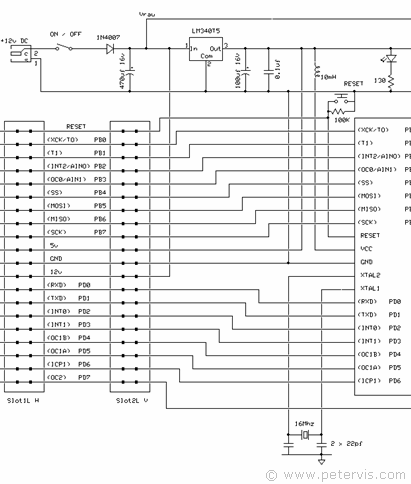

One of the annoying things about this chip is that pin 7 of Port D is on the other side of the chip. This pin had to be re-routed to bring with the rest of the port D pins. As a result, Port D tracks shift up to keep the sequence. I have drawn the schematic like this to make it easier to visualise the board layout where tracks would have to be cut and shifted up as well.
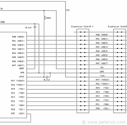
Shifting the pins in this way ensured that I had identical busses on either side of the chip. The voltage rails +5 V, +12 V, and ground are also identical on both sides. There is one slight difference in the busses though. On the RHS sockets, the topmost pin is unused, whilst on LHS it connects to the reset pin. I figure this would be useful if I decide to make a separate ISP connector module.
Power Supply Design Considerations
A good power supply is very extremely critical, and on the oscilloscope, I noticed that the chip draws only a few milli-amperes in short spikes on clock edges. When the I/O lines begin switching, the spikes increase and introduce noise into the power lines. This noise reduces with a decoupling capacitor, however when building on prototyping board it is better to use a 0.1 µF disc, and solder it directly on the Vcc and ground pins on the trackside of the board. The capacitor placing is close to these pins to eliminate any current loops in the power and ground planes. A series inductor also further eliminates this switching noise. A thick coil of around 10 mH that does not create a significant voltage drop works well. I am using a recycled RFI choke. With these two components, the power lines were significantly cleaner. This chip uses a separate voltage supply line for the ADC circuits to eliminate digital noise, and the power line requires decoupling in the same way as the main one.
Reset Circuit
The reset occurs in active low condition, and there is an internal pull-up resistor to establish it to a high. However, in noisy systems, the internal pull-up may not be sufficient and an external pull-up resistor provides further pull-up.
To protect the reset line from RFI noise it is necessary to place a capacitor between reset and ground. In most cases, the internal filtering is sufficient though.
A common mistake students make is to either hard-wire the reset to Vcc or use such a strong pull up that the ISP programmer is unable to enter into programming mode using the reset pin. The pull up resistance should not be less than 4.7 kΩ. In this circuit I am using a 100 kΩ resistor to ground to eliminate noise that would otherwise trigger a reset, and because I plan to use an ISP programming cable.
Resonators and Crystals
It is important to be able to distinguish between a ceramic resonator and a crystal. When you are programming the fuse bits, you will need to select the correct programming options for the component you are using.
A ceramic resonator usually looks like a ceramic capacitor and has three terminals. A crystal is usually in a metal can and has two terminals. A resonator is typically cheaper than a crystal, and has the disadvantage of being more sensitive to temperature and load variations. I am using a 16 MHz crystal, which is easily available from even Maplin. Order Code: RR89.
Circuit Diagram of ATmega32 PORT A and PORT C - RHS
Circuit Board Layout

The circuit board layout may organise in any number of ways, depending upon the ability of the builder and his or her engineering skills. I like pocket size gadgets so I have built this as compact as possible. Building on strip-board can be difficult with a chip of this configuration because not all the Port D pins are on one side. Creating a standard bus was tricky, and I had to shift al the LHS tracks, and in addition move the crystal and capacitor group to the front to make space for the bus.
The thick blue lines represent copper links, whilst the thin blue lines with bends are routed wires. I managed to make this with only three routed wires to get me out of a tight spot, and it saved valuable space. I situated the reset switch and power LED to the front of the board for convenience, and since the board had some space for an ISP header I added that as well.
Parts List
| Parts List | Value |
| C1, C2 | 22 pf |
| C3 | 100 µF / 16 V |
| C4, C5 | 0.1 µF |
| C6 | 470 µF / 16 V |
| Coil | 10 mH |
| LED | Vf = 2.1 V |
| R2 | 130 Ω |
| R1 | 100 kΩ |
| XTAL | 16 MHz |
| Reset Switch | Non-locking push to make |
| D1 | 1N4148 |
| VREG | 7805 |
| DC socket | Barrel Type |
| Header | 6 pin |
| IC1 | Atmel ATmega32 |
Testing
Before you install the main chip, it is very important to test the board first. To begin with, the LED should light up. Check your voltage rails, and make sure there is +5 V and +12 V on the bus, and at all the sockets. Make sure all the ground links are present and showing continuity on a meter. In the future, there might be a forum to provide help, however, until that day comes, keep your ears to the grindstone.
This Article Continues...
ATMega32 Development SystemDevelopment System - Spec
ATMega32 Development Board
ATMega32 LED, Switch, and Sound
ATMega32 Light and Temperature Sensors
ATMega32 Sound Input
ATMega32 UART PC Interface
128x64 Graphic LCD